 


Send e-mail to TAK Corp!

|
 Contact through e-mail is easier! Contact through e-mail is easier!
info@tak-corp.com
Call:+81-53-581-2951 
or send faximili to +81-53-581-2952
 Site renewed on April 30, 2021 Site renewed on April 30, 2021
Laser Diode Line Marker
TAK has developed "Green Laser Diode Line Marker (GLM) " for
variou application. As shown below, the green line with 2mm width can be
projected onto any oblject as shown as a movie and/or indicating simple
line on it.
Laser Marking Application
And the projected beam line is straight so that one can easily find out
level of the structure observed. For lumber factory, the GLM can be used as cutting line marker.
 TAK & B5 Optcs UG in Jena areworking together to boost collaboration
in photonics. TAK & B5 Optcs UG in Jena areworking together to boost collaboration
in photonics.
TAK System started a business using B5 Optics SWIR objective lens.
See through Si wasfer with IR light sourse.
Under the collaboration with B5 Optics in Jena , Germany, TAK System started evaluation of the optics as follows;
■ Specification sheet of the objective lens
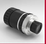 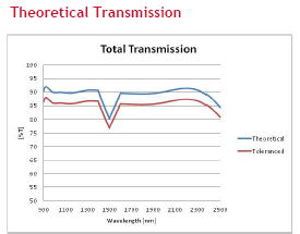
Objective lens and its theoretical transmission spectra
B5 Optcs Data Sheet(English) => 
■ IR imaging experiment using the B5 Optics Objective and a CMOS camera
Using a lamp as a IR light sourse and CMOS camera attached with the Objective,
laser processed line image through the Si wafer was clearly observed.
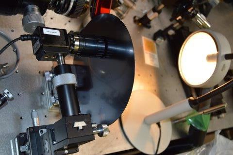 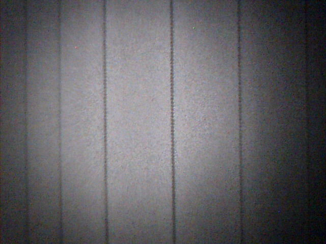
Exp. setup Si processed image
 LIBS (Laser Induced Brakedown Spectroscopy) LIBS (Laser Induced Brakedown Spectroscopy)
By shining laser pulses onto materials and generate laser plasmas, one
can figure out the material compositions from the plasma spectrum. This
is the technique so-called LIBS. We use compact laser system to generate
such plasma and analyse the materials.
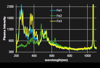
Adopted a ns pulse laser, several kinds ofi irons were irradiated to find
out their plasma spectrum. The spectrum above shows the laser spectrum
at 1.06micron and other material related specific spectrum.
 Special Integration Sphere for agricultural application Special Integration Sphere for agricultural application
Working with Chiba University, TAK System Init. developed a new integration
sphere detection system to be applied for agricultural optical measurment.
Sample reflectyio/transmission can be evaluated using any LED lamp/photometer
system.
 Special LED lamps Special LED lamps
Green and Blue LED lamp for Olympus Microscopes
 Telescopic Photon Counting System Telescopic Photon Counting System
A c-mounted photon counting detector enables very weak optical signal measurements that a sample locates a few meter away from the system.
Why we need such system?
You might need to look at a weak fluorescent sample in a wild field where
it may not be easy to access to it although you can excite it with a laser
beam.
We may use this system to track satellites in space becasue the response of this system reaches to few tens of nanoseconds
that might be good enough to operate the tracking system.
Laser Polarimeter operated at 589nm
Such as, "Polarimeter using D-line laser"
UV transmission measuremnet system
The device contains a compact UV-A to B (290 to 400nm) emission light
source and an integration sphere of 50mm in diameter with a Si photodiode(PD).
First, setting no sample and set light intensity to be "100" on
the output intensity monitor. then set a sample below the white bock of
the integration sphere on the picture, and then observe the "output".
If the output monitor shows "17" then the transmission within
the UV-A and B is easily determined to 17% or the absorption is 83%. The
sample can be thick to 10 mm or so and the sensitivity of the PD can be
selected to higher sensitivity ranges.
Download "UV transmittion measuring system" data.
click ==> 
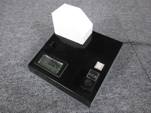
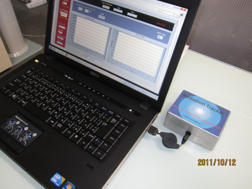
Radiation Tracker
Gamma ray detection system
All data shall be stored into a PC
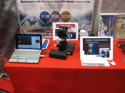
 Hyper-spectral camera Hyper-spectral camera
TAK has developed "Hyper-spectral camera" using a simple transmission grating optics. As shown on the picture below,
we attached a camera lens to the hyper-spectral optics and a color CMOS
USB-camera to observe real time spectral images of what ever it observed
within the spectral range of 300 to 800nm. Since we used 200 micron slit
to select a one dimensional image at the focal point of the input lens,
the spectral resolution was about 18nm.
Download "hyper-spectral camera" data. click ==> 
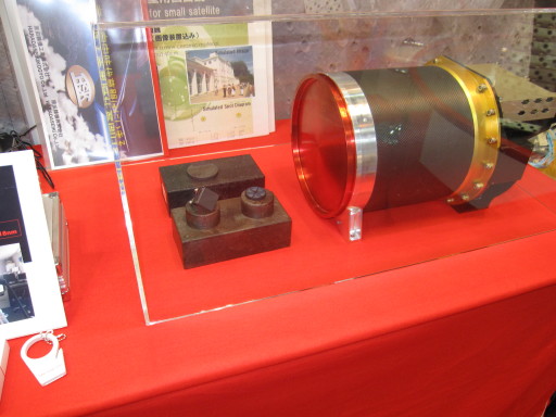
The second one is a "space telescope" adopting zero thermal expansion ceramic mirror at 20 deg.C as shown in
the picture below. A 200 mm dia. spherical concave mirror is the primary
optics in this small telescope at this exhibition. Small mirror samples
were also shown in front of the telescope. 30x30 square one, 30mm dia.
and 50mm dia. flat circle mirrors were displayed. Two circular mirrors'
backs were carved to make them lighter.
Click here for vibration test movie ==> 
Download "Space mirror" data. click ==>
|


■ Borrowing an InGaAs camera from ARTRAY, IR images were obtained with
the objective lens.
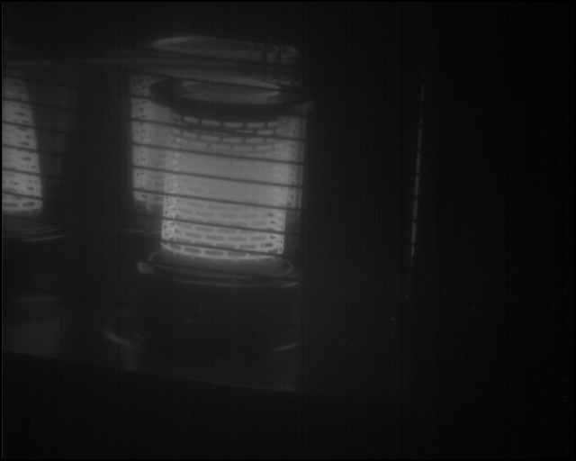
IR image of a stove
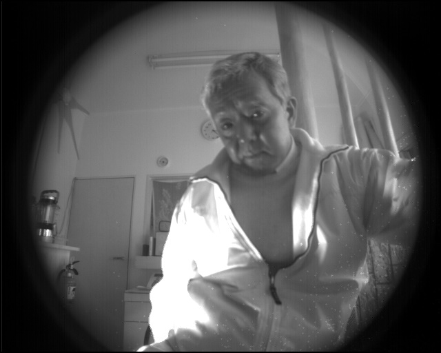
IR image with wide view

Nikon Lens attaced photon counting system
Laser induced fluorescence detection operated at 470 nm laser pumpin
Or "Blue Laser induced Photoluminescence Detection system"
 |
 TAK SYSTEM INITIATIVE CORPORATION